


[Problem Solving] Addressing Dicing Challenges in Package Substrates
As package substrates continue to become denser and thinner, higher precision is increasingly required in back-end dicing processes. In particular, multilayer substrates contain different materials in each layer, making stable cutting more challenging.
This article introduces key challenges in package substrate dicing during semiconductor back-end processing, as well as improvement points made possible with diamond blades.
Key Challenges in Package Substrate Dicing
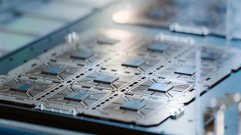
Package substrate dicing is the process of cutting ICs on wafers or packages into individual chips. It is a critical process that directly affects final product reliability and production yield.
Conventionally, dicing machines equipped with high-speed rotating blades have been used for this process. However, maintaining stable cutting performance can be difficult, and defects such as edge chipping may occur on the substrate.
In addition, copper contained in the substrate can adhere to the blade, resulting in reduced cutting ability. Uneven blade wear is also a common issue, leading to shorter tool life, more frequent blade replacement, and lower productivity.
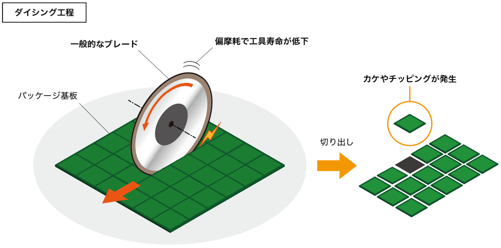
Key issues include:
- Chipping and edge defects on the substrate
- Reduced cutting performance due to copper adhesion on the blade
- Uneven blade wear and shorter tool life
Solving These Challenges with Diamond Blades
Even when using a high-performance dicing machine, the machine’s full capability cannot always be achieved if the blade is not properly selected. This is where Tokyo Diamond Tools’ diamond blades provide an effective solution.
Our diamond blades for package substrate dicing are specially designed for dicing applications, offering both improved cutting surface quality and extended tool life.
The blade edge features our proprietary V-face geometry. This design helps prevent deterioration in cutting performance caused by copper adhesion, while also suppressing chipping and edge defects that tend to occur at the initial stage of cutting.
The blade also offers excellent straight-line cutting performance, helping to prevent uneven wear and maintain stable cutting performance over long operating periods.
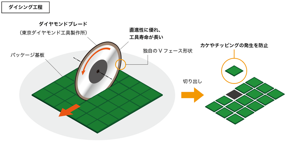
Key improvements include:
- Suppression of chipping and edge defects
- Reduced loss of cutting performance caused by copper adhesion
- Excellent straightness and longer tool life
Recommended Tool for Package Substrate Dicing
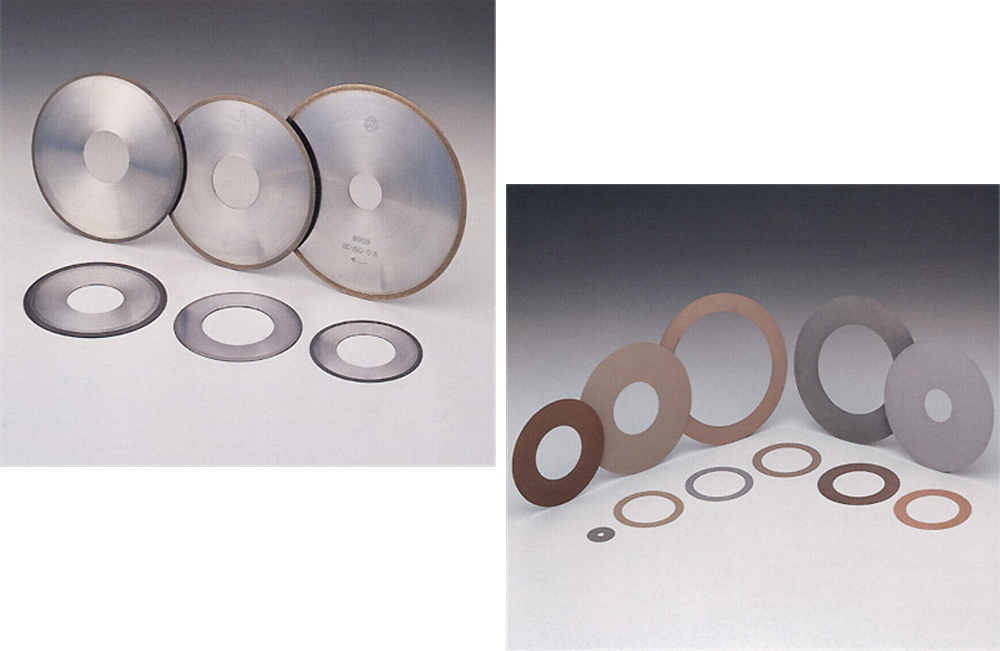
Diamond Blades for Package Substrate Cutting
These are metal bond blades that provide excellent sharpness and high-quality cutting performance. We offer rim-saw type blades with a metal base, as well as all-blade type products.
In addition to package substrates, these blades are widely used for processing multilayer ceramics, magnetic materials, optical glass, and other advanced materials.
Contact Us for a Consultation
In package substrate dicing, even minor chipping or edge defects can have a significant impact on product yield and quality. As substrates become thinner and more multilayered, conventional blades may no longer be sufficient in some applications.
Tokyo Diamond Tools proposes optimal blade specifications according to each customer’s processing conditions, blade outer diameter, blade thickness, and other requirements.
By reviewing blade selection, it is possible to achieve both improved processing quality and longer tool life. We are receiving an increasing number of inquiries from semiconductor manufacturing sites in Japan and overseas.
If you are looking to improve quality and productivity in your dicing process, please feel free to contact us.
