
Longer wheel life in "rough machining" prior to surface grinding of SiC wafers
[Issues in rough machining of SiC wafers]
The production of compound semiconductor wafers, which are used as substrates for power devices, is expected to grow steadily in the trend toward power saving in a low-carbon society. The key to this growth is the processing cost of wafers, which requires a longer wheel life due to the large amount of allowance in the rough machining prior to surface grinding.[Solution with porous vitrified bond wheel]
Our porous vitrified bond wheel "VEGA" has both a larger pore diameter and a higher porosity than conventional wheels, maximizing the biting performance to work materials. It is particularly suitable for surface grinding of SiC wafers and can grind 6" SiC wafers without dressing. The excellent wear resistance increases the number of wafers that can be machined per wheel and contributes to the reduction of wafer machining costs.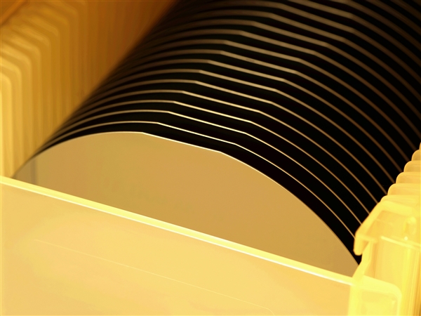
.png)
Wear Rate/Grindability Data of Porous Vitrified Bond Wheel
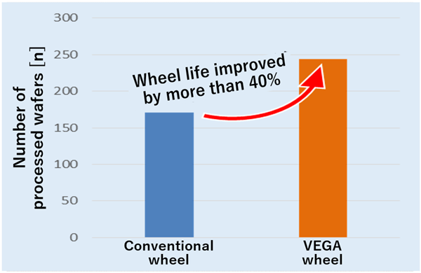
Test machining conditions of wear rate/grindability
Machine : High rigidity grinder
Wheel spec. : #2000 Vitrified bond
Material : 6inch SiC (C)
Optimal grinding tools for processing semiconductor wafers
“VEGA” Porous vitrified bond wheel for compound semiconductor wafers
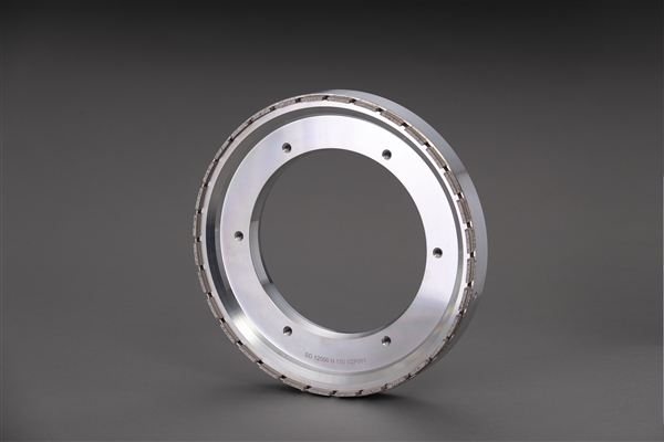
[Product specifications]
Bond : Porous vitrified bond
Grain size : #1000~#3000
[Applied materials]
SiC, GaN, GaAs, LT/LN
■The biting performance to work materials is maximized by both a larger pore diameter and a higher porosity than conventional wheels.
■Spontaneous blade generation is realized and cutting quality is maintained by bonds that can make ultrafine shredding.
■Stable high-quality surface and low processing cost can be realized.